Silicon, as one of important sputtering target raw materials, is mainly used in reaction magnetic control sputtering method to plate SiO2 and SiN and dielectric layers, which has characteristics of excellent hardness, optic and dielectric properties, wear and corrosion resistance as one of important functional film materials. It has wide application in the fields of optics and micro-electronics as the most eye-catching functional material in the international market. Now, it is mainly used in the LCD transparent conducting glass, building LOW-E glass and micro-electronics industries.
Silicon target is classified into monocrystalline and polycrystalline.
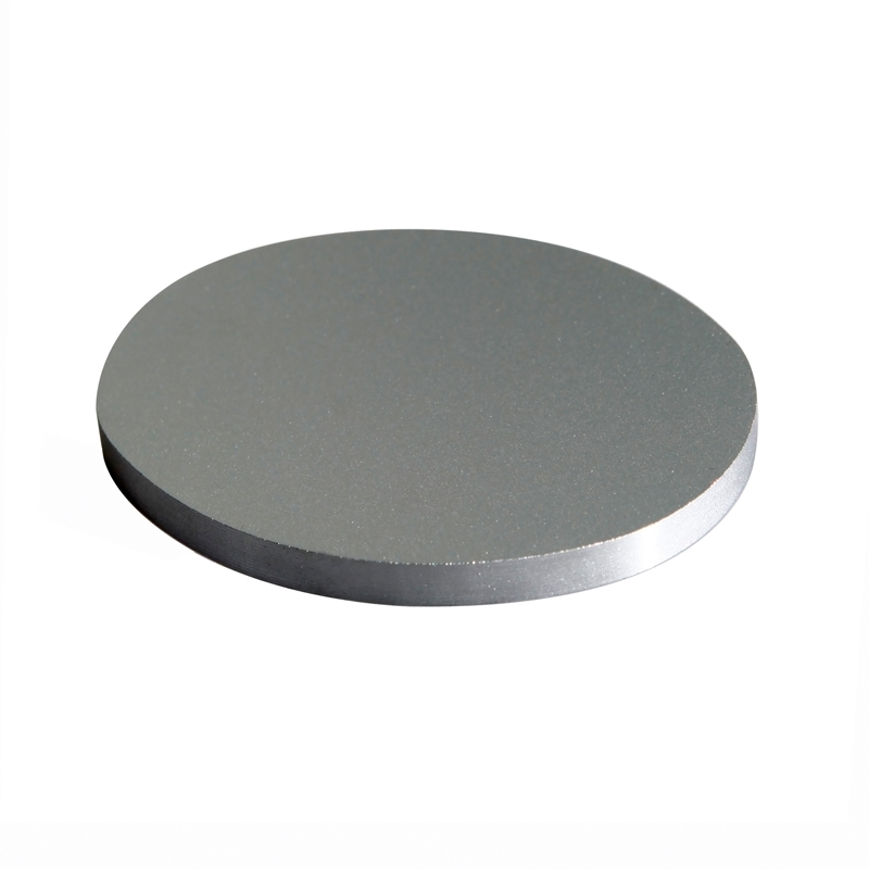
We can produce monocrystalline and polycrystalline silicon targets in the Czochralski crystal growth method, whose crystal particle is uniform, and the diameter can reach 11inch. Silicon targets can be processed into various shapes such as rectangle and round, and can be made in special dimensions according to drawings provided by customers.
Product Specification
Material Purity: > 99.999%
Growth method: Czochralski (CZ)
Crystal orientation: P or N
Content of metal impurities: (Al/Fe/Ca/Mg/Cu/Co/Ni/Cr/Mn/Ti/Na/K//P/W/Mo/Zn/Sn) : <2ppm
L*W: Customization
Thickness: Customization
Planeness (TIR): < 1.2��m
Partial planeness (STIR): <0.3��m
Warp: <30��m